

AMD lifted the hood on its subsequent AI accelerator chip, the Intuition MI300, on the AMD Advancing AI occasion at this time, and it’s an unprecedented feat of 3D integration. MI300, a model of which is able to energy the El Capitan supercomputer, is a layer-cake of computing, reminiscence, and communication that’s three slices of silicon-high and might sling as a lot as 17 terabytes of knowledge vertically between these slices. The result’s as a lot as 3.4-fold increase in pace for sure machine-learning-critical calculations. The chip affords each contrasts and similarities to competing approaches similar to Nvidia’s Grace-Hopper superchip and Intel’s supercomputer accelerator Ponte Vecchio.
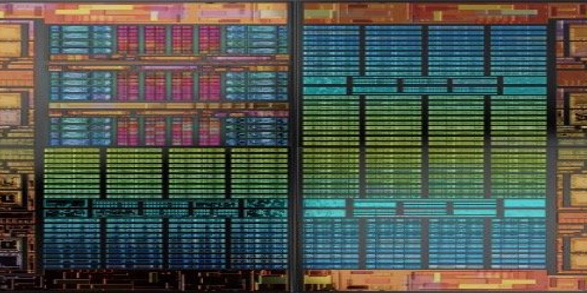
MI300a stacks three CPU chiplets (known as compute complicated dies, or CCDs, in AMD’s lingo) and 6 accelerator chiplets (XCDs) on high of 4 input-output dies (IODs), all on high of a chunk of silicon that hyperlinks them collectively to eight stacks of high-bandwidth DRAM that ring the superchip. (The MI300x substitutes the CCDs for 2 extra XCDs, for an accelerator-only system.) With the scaling of transistors within the airplane of the silicon slowing down, 3D stacking is seen as a key methodology to get extra transistors into the identical space and preserve driving Moore’s Regulation ahead.
Compute and AI chiplets are stacked on high of I/O and cache chiplets within the MI300a.AMD
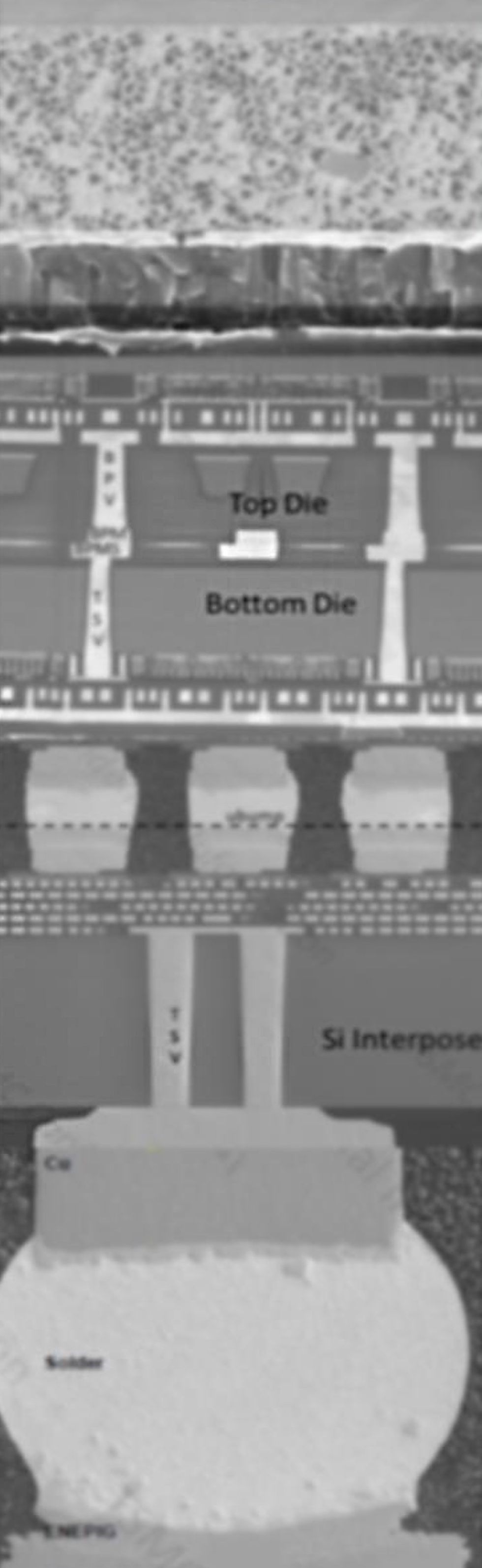
“It’s a really wonderful silicon stack up that delivers the best density efficiency that business is aware of produce presently,” says Sam Naffziger, a senior vice chairman and company fellow at AMD. The combination is finished utilizing two TSMC applied sciences, SoIC (system on built-in chips) and CoWoS (chip on wafer on substrate). The latter stacks smaller chips on high of bigger ones utilizing what’s known as hybrid bonding, which hyperlinks copper pads on every chip instantly with out solder. It’s used to supply AMD’s V-Cache, a cache-memory increasing chiplet that stacks on its highest-end CPU chiplets. The previous, CoWos, stacks chiplets on a bigger piece of silicon, known as an interposer, which is constructed to comprise high-density interconnects.
Similarities and variations between AMD and Nvidia
There are each similarities and variations to chief rival Nvidia’s method. Simply as Nvidia did in its Hopper structure, AMD’s accelerator structure, CDNA3, added the aptitude of computing with truncated 32-bit numbers known as TF32 and with two completely different types of 8-bit floating level numbers. The latter attribute is used to hurry the coaching of sure elements of transformer neural networks, similar to giant language fashions. In addition they each embody a scheme that reduces the scale of the neural community, known as 4:2 sparsity.
One other similarity is the inclusion of each CPU and GPU in the identical bundle. In lots of AI pc methods GPUs and CPUs are individually packaged chips deployed in a 4 to 1 ratio. One benefit to becoming a member of them collectively in a single superchip is that each CPU and GPU have high-bandwidth entry to the identical cache and high-bandwidth DRAM (HBM) in a manner that received’t journey one another up as they learn and write information.
Nvidia’s Grace-Hopper is such a superchip mixture linking the Grace CPU to the Hopper GPU via Nvidia’s Nvidia NVLink Chip-2-Chip interconnects. AMD’s MI300a is as effectively, by integrating three CPU dies designed for its Genoa line and 6 XCD accelerators utilizing its AMD Infinity Cloth interconnect know-how.
However an off-the-cuff look at Grace Hopper and MI300 present some profound variations. Grace and Hopper are every particular person dies that combine all a system on-chip’s wanted useful blocks—compute, I/O, and cache. They’re linked horizontally, and they’re giant—almost on the dimension restrict of photolithography know-how.
AMD took a special method, one which it has adopted for a number of generations of its CPUs and rival Intel used for its 3D-stacked supercomputer accelerator Ponte Vecchio. The idea is named system-technology-co-optimization, or STCO. Meaning, designers began by breaking the chip down into its features and determined which features wanted which manufacturing know-how.

“What we wished to do with MI300 was to scale past what was attainable in single monolithic GPU. So we deconstructed it into items after which construct it again up,” says Alan Smith, a senior fellow and the chief architect for Intuition. Though it’s been doing so for a number of generations of CPUs, the MI300 is the primary time the corporate has made GPU chiplets and sure them in a single system.
“Breaking the GPU into chiplets allowed us to place the compute in essentially the most superior course of node whereas maintaining remainder of chip in know-how that’s extra applicable for cache and I/O,” he says. Within the case of the MI300, all of the compute was constructed utilizing TSMC’s N5 course of, essentially the most superior out there and the one used for Nvidia’s topline GPUs. Neither the I/O features nor the system’s cache reminiscence profit from N5, so AMD selected a cheaper know-how (N6) for these. Subsequently these two features might then be constructed collectively on the identical chiplet.
With the features damaged up, all items of silicon concerned within the MI300 are small. The biggest, the I/O dies, aren’t even half the scale of Hopper. And the CCDs are solely about 1/5th dimension of the I/O die. The small sizes make a giant distinction. Usually, smaller chips yield higher. That’s, a single wafer will present a better proportion of working small chips than it could giant chips. “3D integration isn’t free,” says Naffziger. However the greater yield offsets the associated fee, he says.
Luck and expertise
The design concerned some intelligent reuse of current applied sciences and designs, just a few compromises, and just a little luck, in line with Naffziger, an IEEE Fellow. The reuse got here in two situations. First, AMD was capable of do the 3D integration with a level of confidence as a result of it had already been utilizing the very same pitch of vertical interconnects—9 micrometers—in its V-cache product.
As an optionally available add-on that AMD was capable of cost additional for, V-cache little danger that poor yield or different issues would have a huge impact on the corporate. “It’s been a terrific factor to allow us to ring out the manufacturing issues and all of the design complexities of 3D stacking with out endangering the primary product line,” says Naffziger.
The opposite occasion of reuse was a bit chancier. When the MI300 staff determined {that a} CPU/GPU mixture was what’s wanted, Naffziger “considerably sheepishly” requested the top of the staff designing the Zen4 CCD for the Genoa CPU, if the CCD might be made to suit the MI300’s wants. That staff was beneath strain to satisfy an earlier deadline than anticipated, however a day later they responded. Naffziger was in luck; the Zen4 CCD had a small clean area in simply the appropriate spot to make the vertical connections to the MI300 I/O die and their related circuitry with no disruption to the general design.
Nonetheless, there was nonetheless some geometry that wanted fixing. To make all the inner communications work, the 4 I/O chiplets needed to be going through one another on a selected edge. That meant making a mirror picture model of the chiplet. As a result of it was codesigned with the I/O chiplet, the XCD its vertical connections have been constructed to hyperlink up with each variations of the I/O. However there was no messing with the CCD, which they have been fortunate to have in any respect. So as an alternative, the I/O was designed with redundant connections, in order that irrespective of which model of the chiplet it sat on, the CCD would join.
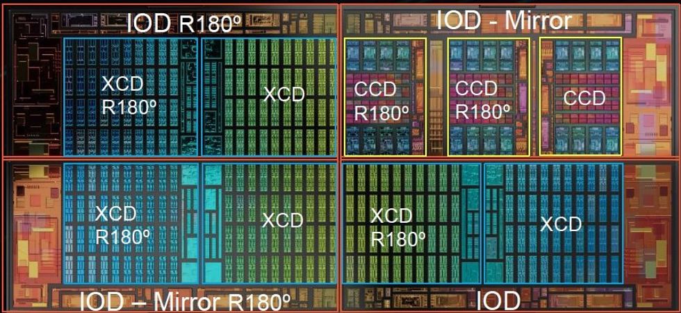

The ability grid, which has to ship a whole bunch of amperes of present to the compute dies on the high of the stack, confronted comparable challenges, as a result of it too needed to accommodate all the varied chiplet orientations, Naffziger famous.
From Your Website Articles
Associated Articles Across the Internet


