


I wish to suppose I can be taught one thing about our readers from the listing of most learn semiconductor articles. What I feel I’ve discovered from this 12 months’s listing is that you’re as obsessed as I’m with packing an increasing number of computing energy into much less and fewer house. That’s good, as a result of it’s the primary purpose of an enormous chunk of the business as properly.
Not all of this listing suits neatly into that mildew, however hey, who doesn’t love a millimeter-scale laser chip that may slice by means of metal?
1971 was a particular 12 months for a variety of causes—the first e-book was posted, the primary one-day worldwide cricket match was performed, this reporter was born. It was additionally the primary time the semiconductor business offered greater than 1 trillion transistors. If TSMC executives’ predictions are appropriate, there can be 1 trillion transistors in only one GPU inside a decade. Simply how the foundry plans to ship such a technological feat was the topic of essentially the most learn semiconductor story we posted this 12 months.
Susumu Noda

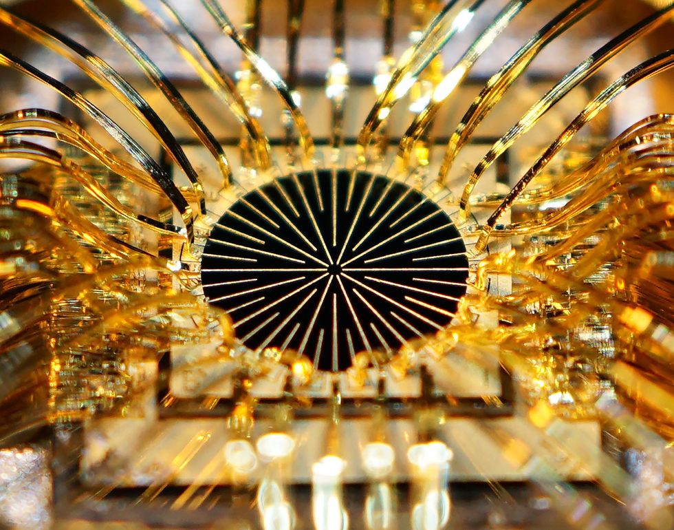
Slicing by means of metal and different feats of optical superheroism have, till very just lately, been the reserve of huge carbon dioxide lasers and equally cumbersome techniques. However now, centimeter-scale semiconductors have joined the membership. Known as photonic crystal semiconductor lasers (PCSELs), the gadgets make the most of a fancy array of rigorously formed nanometer-scale holes contained in the semiconductor to steer extra vitality straight out of the laser. A PCSEL in-built Japan produced a steel-slicing beam that diverges simply 0.5 levels.

Intel had some large ambitions initially of the 12 months. Issues are wanting loads much less rosy now. Nonetheless, the predictions of this January 2024 situation article have come to cross. Intel is ready to fabricate chips utilizing a mix of two new applied sciences, nanosheet transistors and again aspect energy supply. Though the primary competitors, TSMC, is shifting to nanosheets quickly, too, the foundry behemoth is leaving again aspect energy for later. However Intel’s plans didn’t fully survive contact with clients and competitors. As an alternative of commercializing its first iteration of the combo, referred to as 20A, it’s skipping on to the subsequent model, referred to as 18A.

Chris McKenney/Georgia Institute of Know-how

Graphene has lengthy been an attention-grabbing materials for future electronics however a irritating one, too. Electrons zip by means of it at speeds silicon may solely want for, tempting researchers with the potential of terahertz transistors. Nevertheless it has no pure bandgap, and it’s confirmed actually tough to offer it one. However Georgia Tech researchers have given it yet another go and provide you with a reasonably easy technique to make a semiconductor model atop a wafer of silicon carbide.

Intel

Intel’s foundry division is pinning its hopes on gaining foundry clients for its 18A course of, which, as famous above, combines nanosheet transistors and again aspect energy supply. There haven’t been a whole lot of particulars about what clients plan to construct with this tech, however Intel executives did clarify to IEEE Spectrum how they deliberate to make use of these applied sciences, and a few superior packaging too, in a server CPU codenamed Clearwater Forest.


Can anybody beat Nvidia? It’s the subtext of so many articles about AI {hardware}, that we thought we should always ask it explicitly. The reply: A really stable possibly. All of it depends upon what you’re making an attempt to beat the corporate at.

iStock

In a 12 months when the US inked a blitz of preliminary offers as a part of its $52-billion try and reinvigorate its chipmaking business, our loyal readers have been far more concerned about India’s considerably smaller strikes. That authorities introduced a trio of offers, together with the nation’s first silicon CMOS fab. A key architect of India’s plans to spice up chip R&D defined all of it to IEEE Spectrum later within the 12 months.


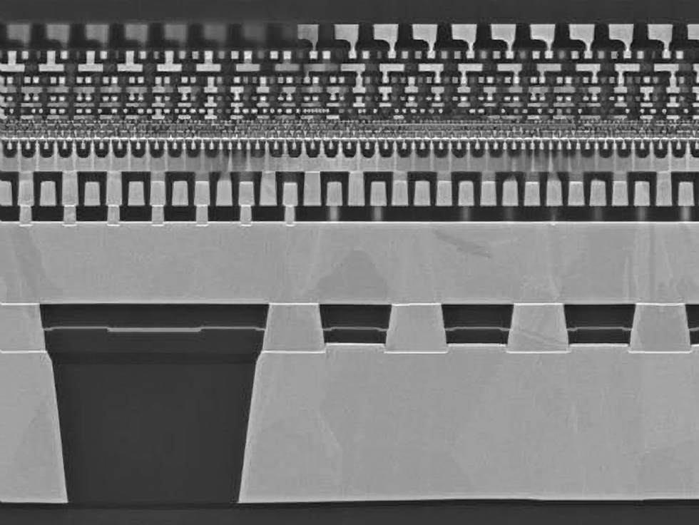
Chip packaging is among the most essential facets of the continuation of Moore’s Regulation, enabling techniques fabricated from many alternative silicon dies linked collectively as in the event that they have been one gigantic chip. And the most well liked factor in superior packaging is a expertise referred to as 3D hybrid bonding. (I do know this as a result of I sat in on at least 20 talks about it on the IEEE Digital Parts Know-how Convention in Could 2024.) 3D hybrid bonding joins chips collectively in a vertical stack with connections so dense you would match tens of millions of them in a sq. millimeter.


Simply once you thought the making of superior chips was already a bonkers course of, right here comes a touch that the longer term can be much more bananas than the current. Excessive-ultraviolet lithography at this time depends on a Rube-Goldberg-esque process of zapping flying droplets of molten tin with kilowatt-class lasers to supply glowing balls of plasma. However future chipmaking will need brighter gentle than such a system may present. The reply, some say, is a big particle accelerator that saves vitality by utilizing the high-energy physics model of regenerative braking.

Tesla

Like cowbell in a sure Seventies rock anthem, future computer systems want extra silicon. How a lot? How about an entire wafer’s filled with it. Again in April, the world’s greatest foundry, TSMC, laid out its plans for superior packaging, and that future factors towards wafer-scale computer systems. TSMC has technically been making one for some time now for Cerebras, however what it’s planning to supply within the coming years can be rather more versatile and universally accessible. In 2027 the expertise may result in techniques with 40 occasions as a lot computing energy as at this time’s
From Your Website Articles
Associated Articles Across the Net


